Explained | Mapping India’s chip design ecosystem Premium
The Hindu
How should policy be tapered to nurture the capital-intensive semiconductor industry? In which area does India have expertise and how can it be leveraged better?
The story so far:
As part of the second phase of the design-linked incentive (DLI) scheme for the domestic semiconductor industry, the Indian government, according to media reports, is considering a proposal to pick an equity stake in domestic chip design-making companies. The modalities and the timing of the policy are yet to be worked out, but senior government officials say the idea behind the scheme is to ensure a stable ecosystem alongside building a few “fabless companies”. (Fabless companies are entities that design chips but outsource the manufacturing.)
Any policy directed towards the semiconductor industry, be it manufacturing, or design, requires a long-term strategy as the sector is capital-intensive and involves sizeable costs in setting up fabrication units, upscaling manufacturing capabilities and equipment (such as thermal stimulators, sensors), and pushing research. Moreover, returns from the investment are not immediate as setting up design and fabrication units involves long gestation periods.
Also read | India’s semiconductor market to reach $55 billion by 2026: Deloitte
Industry body NASSCOM says it takes up to 2-3 years before the first product is out and chip designing requires higher investment than a traditional aggregator company. Further, as chipsets become smaller and functional requirements from them change, research and development become challenging in an already cyclic industry. Lastly, supply chain disruptions, like what happened during the COVID-relatedlockdowns in China, could dampen potential investor confidence in the sector.
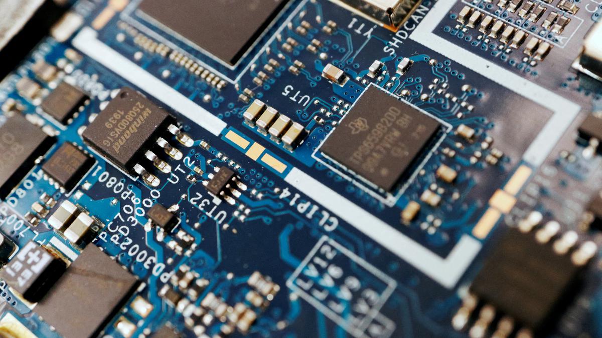
India is an important destination for global semiconductor companies primarily because of its highly-skilled talent pool of semiconductor design engineers, who make up about 20% of the world’s workforce as part of global teams or working independently. About 2,000 integrated circuits and chips are designed in India every year with engineers involved in varied aspects of design and verification. Global players operating R&D in the country include Intel, Micron and Qualcomm among others.
Notwithstanding the thriving manpower, India owns a much smaller portion of the intellectual property (IP) relating to the designs, which are mostly retained by the global companies. The DLI for chip designing introduced in December 2021 endeavoured to indigenise innovations. Among other things, it aspired to grow at least 20 companies in India scaling a turnover of more than ₹1,500 crore in the next five years. For product design, the scheme will reimburse up to 50% of the eligible expenditure to a ceiling of ₹15 crore per application. The deployment-based support, meaning using it in electronic products, extends the incentive by 4-6% of net sales turnover at an upper limit of ₹30 crore per application.

The rupee declines 20 paise to 93.73 against the dollar as global oil prices rise and investor uncertainty persists.

Siemens said on Monday that the Iran war has led to customers holding back on new investments as prices increase for raw materials and energy.

OpenAI said its close ties with Microsoft could be a potential risk to its business, telling investors that the software company is responsible for “a substantial portion of our financing and compute,” CNBC reported

LPG crisis: Alternative solutions are being considered, with ammonia cylinders being increasingly used for industrial applications amid delays in commercial LPG deliveries.

India monitors U.S. military pause on Iran as oil prices dip; External Affairs Minister engages with GCC nations for support.

India monitors U.S.-Iran tensions as Trump pauses attacks, leading to a significant drop in oil prices.

Union Minister Ashwini Vaishnaw launches three initiatives to enhance India's creative economy through AI training, citizen platforms, and advanced tech access.

Two Indian-flagged LPG tankers approach the Strait of Hormuz, navigating safely amidst regional tensions to reach Indian ports.

Gold and silver prices plummet over 7% due to West Asia tensions, inflation fears, and a stronger dollar.

Asian shares fall as rising oil prices and escalating Iran conflict diminish hopes for U.S. interest rate cuts.

Japan's SoftBank Group said Saturday it plans to build a huge new gas-fired power plant in the US state of Ohio

Silver prices plunge 9% to ₹2.06 lakh per kg in futures trade amid weak global cues and rising macroeconomic pressures.

OpenAI plans to nearly double its workforce to 8,000 from 4,500 by the end of 2026, the Financial Times reported on Saturday, citing two people with knowledge